ENGINEERING
The 1947 Transistor and the Art of Controlling a Larger Current
The first transistor made semiconductor amplification practical. Its original papers reveal how bias, surfaces and power gain shaped an engineering landmark.
Research checked
Newest cited publication
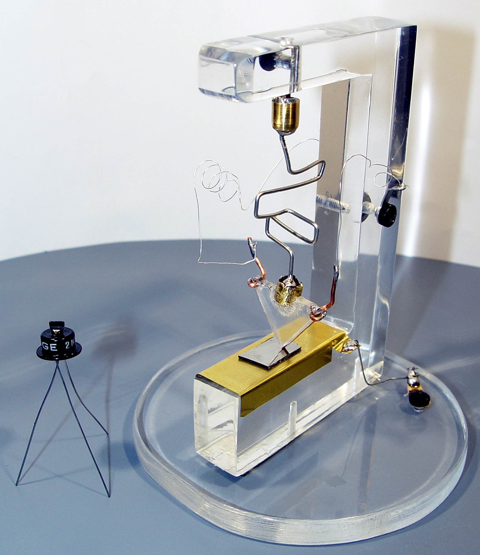
A replica of the first working point-contact transistor appears beside a 2N43 transistor in a 2019 photograph. The replica supplies physical context for the 1947 breakthrough.
Mister rf / Wikimedia Commons · Image source · CC BY-SA 4.0

A useful amplifier lets a faint signal influence something more energetic: a telephone conversation can drive a distant receiver, or a small electrical variation can become a measurable output. The transistor demonstrated at Bell Laboratories in December 1947 brought that possibility into a solid piece of semiconductor. Understanding the achievement requires more than noticing its size. The revealing questions concern where the output energy came from, how two nearby contacts influenced one another, and what evidence separated genuine amplification from a convenient change in resistance. The original engineering record offers unusually clear ways to ask those questions.
A telephone network needed dependable control
Bell Labs' institutional account places the research within the search for alternatives to telephone-network relays and vacuum tubes. Relays could switch signals but introduced mechanical constraints; tubes provided electronic amplification with their own operating and reliability burdens. John Bardeen and Walter Brattain's subsequent paper acknowledges William Shockley's direction of the research program. These were related contributions, rather than evidence that every stage of the device's development belonged to an interchangeable group. The point-contact experiment and the later junction concept deserve their own explanations.
Consider the design brief from the viewpoint of an engineer responsible for many unattended amplifiers. A component must work at its specified temperature, survive handling, and behave similarly enough to its replacement that the surrounding circuit remains useful. A spectacular laboratory response establishes an opportunity, but dependable service demands an operating envelope. This distinction helps explain why a first demonstration matters without treating it as a finished network product. The engineering question becomes whether a controllable physical effect can be packaged, characterized and reproduced with manageable variation. That is a larger assignment than simply shrinking an existing circuit.
Two nearby contacts changed the problem
The July 1948 Physical Review report describes germanium with two closely spaced point contacts, called emitter and collector, and a larger low-resistance base contact. A small forward bias at the emitter and a reverse bias at the collector produced a coupled response. The authors interpreted the injected charge mainly in terms of holes, which act as positive mobile carriers. Varying the emitter signal changed the collector current. Crucially, the operating circuit could supply power gain; it was doing more than measuring how a lone metal contact conducted in one direction.
An electrical device with three connections permits an important division of responsibilities. One connection can help establish a reference, while the other two participate in input and output circuits. Their interaction allows the input to influence energy delivered elsewhere. Calling those roles input and output is a circuit-level choice: the physical terminals themselves still belong to one interacting object. Consequently, a datasheet must describe the chosen connection and bias conditions. A gain value without that context can disguise important differences between two experiments, even when both experiments use a component called a transistor.
Power gain needs an energy account
The original paper reports measured amplification and also discusses feedback that could make some operating conditions unstable. An amplifier therefore needs more than a large output excursion: its useful response must remain controllable. Here is an illustrative calculation, using invented circuit values rather than measurements of the 1947 specimen. Suppose an input delivers 4 millivolts root mean square across an effective resistance of 1,000 ohms. Applying power equals voltage squared divided by resistance gives 16 nanowatts. An output of 40 millivolts across 10,000 ohms supplies 160 nanowatts. The voltage ratio is ten, while the power ratio is also ten in this particular example.
Changing the output resistance would change the power comparison even if both displayed voltages stayed the same. That is why voltage amplification alone cannot establish that a device delivers additional signal power. The extra energy in the example must come from a separate supply; the signal governs its delivery. Measuring supply current alongside input and output power closes the accounting. It also exposes an amplifier that obtains attractive gain by consuming unacceptable standing power. The useful result is controlled energy transfer, subject to noise, distortion and stability requirements.
The surface belonged inside the explanation
Bardeen and Brattain's patent describes a semiconductor body, emitter, collector and base, with operation depending on the material, its surface and applied potentials. Its discussion includes carrier injection and the collector's influence near the emitter. The experimental paper also records surface preparation and carefully presents parts of its carrier picture as an interpretation. Reading that language matters: a working result can precede a complete account of every microscopic contribution. A historical explanation should preserve that distinction rather than lending the first experiment knowledge developed afterward.
A useful independent way to think about sensitivity is to imagine two nominally identical contacts whose local environments differ. The circuit diagram treats them as the same symbol, yet their boundary conditions may differ because of handling, processing or geometry. An engineer can test this by varying one preparation step while holding the bias and measurement procedure fixed. Repeating the experiment across multiple samples then distinguishes a systematic treatment effect from an unusually favorable specimen. The point is methodological rather than a proposed reconstruction recipe: the physical device includes its interfaces, even when a simplified diagram draws only three wires and a block.
A junction transistor changes the design task
Shockley's patent, filed in June 1948 and published in September 1951, develops semiconductor regions and barriers whose conduction can be controlled through charge carriers. This junction-based route is physically distinct from pressing two point contacts against a prepared surface. An explanation that silently substitutes the later structure for the December 1947 device loses the very engineering transition worth understanding. The newer arrangement moved critical questions toward the dimensions, conductivity types and carrier behavior of regions inside a semiconductor body.
For an illustrative design argument, imagine injected carriers moving toward a collecting region while some disappear through recombination. A longer effective journey creates more opportunity for loss; a geometry that shortens the journey can improve collection, assuming other conditions remain suitable. But making regions smaller also makes dimensional variation a larger fraction of the intended dimension. If a hypothetical region should be 10 units thick, an error of one unit is ten percent; at two units, the same error is fifty percent. Those arithmetic examples describe a manufacturing tradeoff, not historical device dimensions. Better physical control and better process control must develop together.
The landmark is a sequence of stronger claims
The patent records and experimental paper support different kinds of conclusions. A patent describes an invention and its proposed embodiments; a measured paper reports behavior obtained in specified circumstances. Neither automatically tells a reader how many production devices passed inspection or how a network performed after years of service. Keeping those evidence levels separate allows the first transistor to remain a remarkable result without making it responsible for proving every later commercial achievement. The surviving documents also show why attribution should follow particular experiments, explanations and designs.
A good modern reading exercise is to write a claim ladder before evaluating any new amplifier. First ask whether a reproducible response exists. Then ask whether signal power increases, whether the response remains stable, and whether different specimens meet the same specification. Finally ask what happens after integration into the intended system. Each step needs a different experiment and may reveal a new limitation. The 1947 transistor opened a particularly consequential path through that ladder. Its lasting engineering lesson is the discipline of turning a controllable physical interaction into a component whose behavior another engineer can confidently use.
Sources & further reading
Primary papers, project documentation, and research releases used in this article. Publication dates below refer to the sources themselves.
- The Transistor, A Semi-Conductor TriodeJ. Bardeen and W. H. Brattain / American Physical SocietyPublished Checked
- US2524035A: Three-electrode circuit element utilizing semiconductive materialsJohn Bardeen and Walter H. Brattain / United States Patent Office, hosted by Google PatentsPublished Checked
- US2569347A: Circuit element utilizing semiconductive materialWilliam Shockley / United States Patent Office, hosted by Google PatentsPublished Checked
- 1956 Nobel Prize in PhysicsNokia Bell LabsChecked
FOLLOW THE QUESTION
Explore engineering