ENGINEERING
Getting Light Off the Chip: Silicon Photonics Meets Real Packaging
A 2026 optical-I/O prototype and recent polymer-waveguide experiments expose how mode matching, polarization, and assembly decide usable photonic performance.
Research checked
Newest cited publication
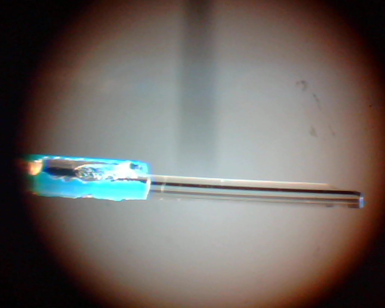
A microscope image of optical fiber provides context for coupling light between a chip and an external link; the damaged fiber shown is a structural illustration.
Stalinets / Wikimedia Commons · Image source · CC BY-SA 4.0

A photonic chip is useful only when light can enter, leave, and reach the intended receiver without losing too much power. That mundane requirement becomes difficult when a tightly confined on-chip optical field must connect to a much larger fiber, or when a laser made from another semiconductor has to align with a silicon-based platform. Recent experiments address those interfaces directly. A February 2026 preprint reports an optical input/output prototype on a silicon-oxynitride interposer. A March 2025 paper studies polymer waveguides connected to silicon-nitride structures. Both show why packaging belongs inside the optical design, rather than being treated as a final container.
An optical connection joins fields, not just visible edges
Light in a waveguide occupies a spatial electromagnetic mode. Two components can look aligned under a microscope while their optical fields overlap poorly. A fiber mode may spread across several micrometres, while the field in a strongly confining integrated waveguide is much smaller. Simply placing the facets opposite each other can send a substantial fraction of the optical power into unwanted directions or modes. Engineers therefore shape the field gradually, or use an intermediate material, before asking the two interfaces to exchange light efficiently.
An independent analogy is a doorway between rooms of very different widths: aligning their centers does not ensure that every path through the wider room enters the narrow opening. The actual optical calculation involves field overlap rather than rays alone. Polarization, phase, and refractive-index structure all matter. An efficient converter must preserve the intended guided field while avoiding radiation and unwanted higher-order modes. This is why the smallest footprint is not always the best interface. A longer transition can buy manufacturing tolerance that a very abrupt transition lacks.
Alignment tolerance should be specified in more than one direction. Lateral displacement changes field overlap, vertical separation changes coupling strength, and angular error can accumulate along an extended interface. A tolerance measured by shifting only one axis may overestimate the window available when several errors occur together. Engineers can build a response surface from deliberately displaced samples and then compare it with the assembly machine’s measured error distribution. That turns an attractive best-case transmission into a prediction that can be checked against production-like placement variation.
What the February 2026 prototype actually demonstrated
Daibao Hou and colleagues submitted their silicon-oxynitride/silicon optical-interposer study on February 9, 2026. The preprint describes flip-chip integrated indium-phosphide active devices, electronic drivers and receivers, and passive wavelength routing. It reports four optical channels at a nominal 100 gigabits per second each. The receiver error measurements explicitly test channels without interference from the other channels. That qualification matters: the reported experiment should not be retold as a comprehensive simultaneous-channel production qualification.
The material choice divides responsibilities. Passive routing does not need to be made from the material that generates light most efficiently, and the driver electronics need not use the same device physics as the laser. Heterogeneous integration tries to connect components that are individually suited to their roles. Its price is additional interfaces. A system may gain a better laser and a more forgiving optical route while creating new alignment, reflection, electrical-contact, and heat-removal problems between them. The design is successful only if the complete collection works better than the alternatives.
A polymer waveguide can become part of the package wiring
Jef Van Asch and colleagues’ March 4, 2025 manuscript investigates two ways of joining silicon-nitride waveguides to package-level polymer waveguides. One patterns the polymer on the photonic chip; the other uses a flip-chip arrangement. Their experimental results report coupling losses around one decibel for both principal polarization orientations in the optical O-band. The work is a measured integration demonstration, with a related Optica publication linked from the research record; it does not by itself establish high-volume assembly reliability.
A taper changes the geometry gradually so that a guided mode can evolve from one structure into another. The word adiabatic in this setting refers to that gradual evolution, not to thermal insulation. Making the change too abruptly can scatter energy or excite an unwanted mode. Making it longer consumes area and may add propagation loss. The engineering optimization therefore balances transition length, field overlap, fabrication variation, and the rest of the package layout. A design with slightly higher nominal loss can be preferable if it remains usable across a much wider alignment window.
Decibels make a connection budget easier to audit
Optical losses accumulate multiplicatively in power, while their decibel values add. In a worked example, suppose a route contains a one-decibel chip transition, a one-decibel connector, and a two-decibel passive circuit. The total is four decibels. The transmitted power fraction is approximately 10 raised to minus 0.4, or 0.398. Thus about 40% of the original power remains before any further losses. These assumed numbers are educational examples, not a reconstruction of either reported experimental platform.
That calculation also explains why a small interface improvement can matter. Reducing the total loss from four to three decibels increases the surviving fraction from about 40% to about 50%. It does not automatically lower total system electricity by the same percentage. A laser’s electrical efficiency, fixed control power, receiver sensitivity, and operating margin remain relevant. Engineers should keep the optical budget separate from the electrical-power budget, then connect them through a clearly stated model. Otherwise a better coupler can be turned into an unsupported claim about an entire data center.
The reference measurement decides what the loss number means
A measured transmission includes the component under study and every other element between the light source and detector. Researchers therefore use reference structures, calibration, and repeated measurements to isolate the intended contribution. If two nominally identical transitions sit in series, dividing the combined excess loss by two requires an assumption that their contributions are comparable. Propagation loss must be estimated separately, and reflections can make a simple additive interpretation inaccurate if they produce wavelength-dependent interference.
The same care applies to polarization and bit-error measurements. Testing several polarization settings is useful evidence, but it is different from continuously exploring every possible state over a wide temperature range. Measuring a favorable channel alone does not reveal the effects of every neighboring channel operating simultaneously. A complete qualification plan would vary wavelength, alignment, temperature, power, and activity pattern, while retaining enough information to identify which interface caused a failure. The paper’s stated measurement boundary is often more valuable than a rounded headline about aggregate speed.
A larger optical mode can make one interface more tolerant while making another part of the route harder. Weakly confined light generally requires more care around tight bends and nearby structures because the field extends farther from the nominal waveguide core. Routing density, bend loss, and unwanted coupling must therefore be evaluated along with facet alignment. The optimum material stack is a balance across the whole optical path. Improving a single interface by enlarging its mode is useful only if the subsequent layout retains adequate separation and manageable curvature.
From an attractive interface to an assembly process
TSMC’s current SoIC documentation identifies its compact universal photonics engine, COUPE, among ongoing integration developments. That provides industrial context for the research, without proving that the particular polymer or silicon-oxynitride interfaces discussed here are adopted in that platform. A March 2026 architectural perspective by Yi and Wilkerson similarly argues for treating optical integration as a coupled system-design problem. Such context can guide questions, but the experimental papers remain the evidence for the specific measured devices.
My practical conclusion is to evaluate an optical interface as a manufacturing window rather than a single best alignment point. A useful process should tolerate realistic displacement and material variation, retain its behavior after bonding and temperature cycling, and expose test points before the most expensive assembly steps. The emerging choice is not simply between electricity and light. It is between ways of joining materials, fields, and electronics with enough repeatability to make the communication link dependable. The 2025 and 2026 experiments are valuable because they turn that joining problem into measurable engineering.
Sources & further reading
Primary papers, project documentation, and research releases used in this article. Publication dates below refer to the sources themselves.
- 2.5D co-packaged optical I/O chipsets on a SiON/Si interposer for 4 × 100G optical interconnectionarXivPublished Checked
- Low-Loss Integration of High-Density Polymer Waveguides with Silicon Photonics for Co-Packaged OpticsarXivPublished Checked
- TSMC-SoIC®TSMCChecked
- 3D optoelectronics and co-packaged optics: when solving the wrong problems stalls deploymentarXivPublished Checked
FOLLOW THE QUESTION
Explore engineering